Thankyou so much for your guidance. I will try!
Chhatra
@Chhatra
Posts
-
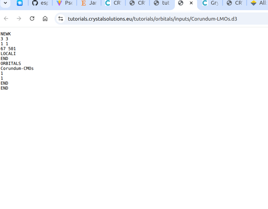
Localized Crystalline Orbitals -
Localized Crystalline OrbitalsThank you for your reply—it has been very helpful.
I am currently trying to obtain the crystalline orbitals for a 7×7 supercell of MXene with a dye adsorbed on it. However, the generated .molden file for just gamma point is quite large (around 1.4 GB). I have attempted to open it using Jmol, even allocating up to 40 GB of RAM, but it still does not load.
Could you please advise on how to proceed with handling or visualizing such a large file?
-
Localized Crystalline Orbitals -
Plotting band-decomposed charge density (CBM/VBM) for 2D Janus monolayer -
Plotting band-decomposed charge density (CBM/VBM) for 2D Janus monolayerThank you very much for your previous help — the method works perfectly for the valence band.
However, I’m encountering an issue when trying to plot the partial electron density for the conduction band. It does not seem to return any values, possibly because those bands are unoccupied.
I was wondering if there is an alternative way to analyze the conduction band states — for example, accessing the corresponding wavefunctions or something analogous to HOMO/LUMO analysis in molecular codes like Gaussian.
Any guidance or suggestions would be greatly appreciated.
Thank you in advance!
-
Plotting band-decomposed charge density (CBM/VBM) for 2D Janus monolayer -
Plotting band-decomposed charge density (CBM/VBM) for 2D Janus monolayerDear Crystal Users and Developers,
I am currently studying the electronic properties of a 2D Janus monolayer, using CRYSTAL17. I am interested in visualizing the spatial localization of the Valence Band Maximum (VBM) and Conduction Band Minimum (CBM) to confirm charge separation across the Janus surfaces.
My system is a semiconductor with a direct band gap at the
K point. I would like to generate 3D electron density maps (isosurfaces) for these specific bands only.Any guidance or example .d3 inputs for band-specific density plotting would be greatly appreciated.
Thank you for your time and help.Best regards,
Chhatra Subba -
Band Edge Alignment -
Band Edge AlignmentThank you so much for your response. I tried it, but it shows an error
GCALCO - MAX INDICES DIRECT LATTICE VECTOR 29 29 3
NO.OF VECTORS CREATED 6999 STARS 3500 RMAX 122.19169 BOHR
TTTTTTTTTTTTTTTTTTTTTTTTTTTTTT gordsh1 TELAPSE 0.05 TCPU 0.02MATRIX SIZE: P(G) 377103, F(G) 76624, P(G) IRR 193585, F(G) IRR 78287
MAX G-VECTOR INDEX FOR 1- AND 2-ELECTRON INTEGRALS 321CAPPA:IS1 8;IS2 8;IS3 8; K PTS MONK NET 260; SYMMOPS:K SPACE 2;G SPACE 1
PLANE AVERAGED ELECTROSTATIC POTENTIAL
N. OF POINTS 201 ZMIN -20.000 (AU) - ZMAX 20.000 (AU)
**** LDIM, ICASO= 4 2
ERROR **** POTCAL **** CASE NOT AVAILABLE
Abort(1) on node 2 (rank 2 in comm 0): application called MPI_Abort(MPI_COMM_WORLD, 1) - process 2Does this method only work for SLAB systems created using CRYSTAL17’s SLABCUT utility or SLAB keyword used in input geometry block? My present work involves a 2D material slab, but I generated the slab structure using VESTA and modeled it in CRYSTAL keyword in input block with a 15 Å vacuum along the z-direction
-
Band Edge AlignmentDear CRYSTAL developers and users,
I would like to perform a band edge alignment calculation by referencing the valence/conduction band edges to the vacuum level in the context of photocatalysis. For this purpose, I need the planar-averaged electrostatic potential along the slab normal direction.
I have already generated the electrostatic potential in Gaussian cube format using the POTCUBE keyword (file: POT_CUBE.DAT).
My questions are:
Does CRYSTAL provide any direct tool or utility to compute the planar average of the electrostatic potential from POT_CUBE.DAT (or other related output files)?
If not, is it recommended to post-process the cube file externally (e.g., with scripts, VESTA, or custom Python routines)?
Any guidance, example workflows, or scripts would be greatly appreciated.
Best regards,
Chhatra Subba -
Generatinng INPUT file for difference map of electron charge density and electrostatic potential plot -
Generatinng INPUT file for difference map of electron charge density and electrostatic potential plotDear Developer,
I have referred to the user manual and tutorial materials, but I am still having difficulty understanding how to correctly define the following sections when generating 2D electron density and electrostatic potential plots using CRYPLOT (Specifically following section)
'''''''''''''
ATOMS
1 1 1 -1
1 0 0 0
1 0 0 2
MARGINS
2. 2. 2. 2.
END
''''''''OR
'''''''''''
COORDINA
-2.498 0.000 1.696
-2.498 0.000 -1.696
-1.249 -2.164 -1.696
RECTANGU
MARGINS
3. 3. 3. 3.
'''''''''Could you kindly explain how to determine or generate these inputs properly?
Thank you very much for your assistance.
Best regards,
Chhatra Subba -
Conversion of fort.25 file to .cube (Vesta file) -
Conversion of fort.25 file to .cube (Vesta file)Thank you for your response.
The procedure worked perfectly for the 3D structure. However, I'm encountering difficulties when applying it to a 2D system. Specifically, after using the SLABCUT option and optimizing the structure, the same plotting method doesn't seem to work as expected.Could you kindly guide me on how to correctly generate the 3D charge density for a 2D slab model?
I got this error
DENSITY MATRIX - CONTRIBUTION FROM BANDS
22 23
WARNING **** PDIBAN **** K POINTS WEIGHTS MODIFIED - COMPTON PROFILES NOT ALLOWED
TTTTTTTTTTTTTTTTTTTTTTTTTTTTTT PBAN TELAPSE 0.02 TCPU 0.02
ERROR **** GRID3D **** OPTION NOT ALLOWED
TTTTTTTTTTTTTTTTTTTTTTTTTTTTTT ERR TELAPSE 2.02 TCPU 0.02Regards
Chhatra Subba -
Conversion of fort.25 file to .cube (Vesta file)I am a new user of CRYSTAL17. I successfully completed a properties calculation and obtained the file fort.25, which I can visualize using CRYPLOT. However, I would like to plot the charge density in VESTA, and currently I'm not sure how to convert the output to a compatible format.
Could you please guide me on how to:
Convert fort.25 to a Gaussian CUBE file or any other format supported by VESTA?
Specify the correct options using runprop17 (or any other utility) to export the 3D total charge density?Any help would be greatly appreciated.
Best regards,
Chhatra Subba